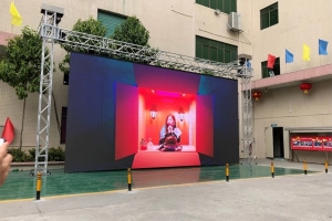
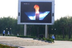
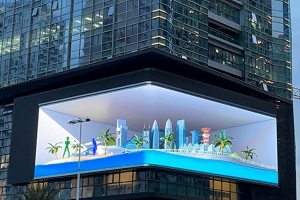
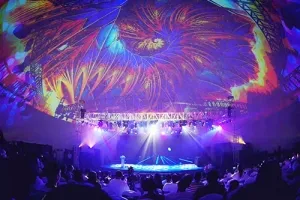
As a display product with high engineering and customization, LED display screens are mostly outdoor large screens at the beginning. The image appears near the landmarks such as the surface of the building and the square, but as the dot pitch of LED display products goes from PXX to PX and then breaks through P1, and continues to march toward PO.X, LED display products begin to be used indoors The direction continues to infiltrate. In the early era of large outdoor screens, the “distance” between users and users getting closer as the distance between dots continues to decline. Whether it is Samsung’s entry into LED movie screens or the construction of electric stadiums and LED display manufacturers, The mutual achievement of each other illustrates this point.
Therefore, the controversy over whether “developing smaller-pitch LED display products has practical significance” was clearly settled: For LED display manufacturers, the dot pitch is getting smaller and smaller, which is that LED displays can penetrate the indoor market and expand more Difficulty in the multi-divided field is actually a sense of shrinking the foundation of production. On the eve of the era of “5G + 8K”, the interactivity of LED displays is only possible when the dot pitch is getting smaller and smaller.
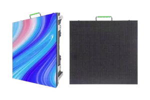
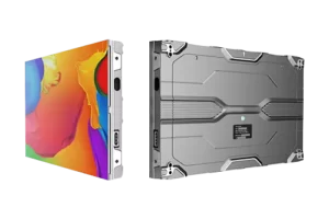
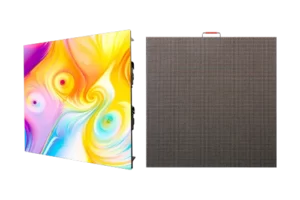
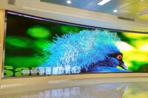
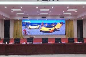
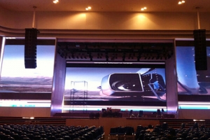
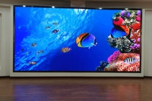
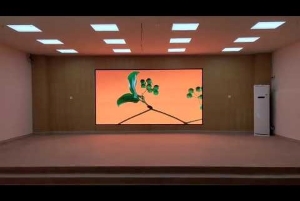
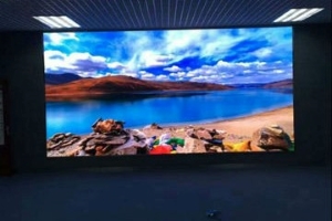
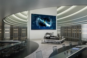
Indoor LED Display Panel
The development and maturity of the indoor fixed led display have shortened the distance between the LED display and the audience. When the screens of LED display products start to become more and more clear, how to further reduce the distance with the user, so that the LED display and the User interaction has become an issue that manufacturers must consider.
Although LED display has the advantages of fast response speed and high dimensional freedom, compared with other display methods, it is more difficult for LED display to achieve touch interaction than touch display technology. Other technologies: For the Indoor LED Display Screen to achieve interaction, it is necessary to reduce the dot pitch as much as possible, so that even when the picture is viewed at a close distance, there is still no obvious “graininess”.
But as the dot pitch decreases, it will inevitably face For the stability and safety problems caused by the shrinking of the solder pins, for the LED display base to have a real display, as a discrete device assembly product, the LED display product has stability in comparison with other display products. “Congenital deficiency”, even bumps during transportation may cause the display of the screen to malfunction.
Therefore, at this stage, many Indoor LED Display panels often intentionally make a “No touch on touch” mark during exhibition and use. It is because when the audience touches it, it is very easy for the sweat and grease secreted from the fingers to be left on the screen, causing a short circuit and a hidden danger of reducing the life of the lamp beads. Some static electricity may even cause an electrostatic breakdown.
Therefore, it is conceivable that the touch caused by the audience’s touch interaction is obviously stronger and more frequent than the collision during transportation. In terms of touch screen, the pace of LED display is always slower than other display methods. Although some manufacturers choose to solve the above problems by laminating the screen surface, in general, how to solve a series of problems such as dead lights, bad lights, short circuits, and electrostatic breakdown caused by touch, Indoor LED Display Screen companies have a long way to go.
However, with the advent of the “5G + 8K” era, ultra-high-definition video display and ultra-high-speed signal transmission will inevitably put forward higher technical requirements for display products, and this will also necessarily include increased requirements for touch ability. And if you want to make the display at your fingertips, “the first thing to consider is how to improve the stability and security of the screen.
At present, the types of LED packages in the market are different. The most common Nin1SMD (4in1 / 6in1) products are an extension of the SMD technology line and a transition product of traditional SMD production plants. This product is still used SMT technology to paste Installation, using 41n1 lamp beads, the distance between the edge of the lamp beads and the internal solder joints is about 0.1mm, the core issues such as the airtightness of the lamp bead edges, and the exposed solder pins have not been fundamentally solved. Come out and have not been effectively improved. Under normal conditions, a gap of 0.25mm needs to be reserved between the lamp beads, and the discrete device size specifications, basically can not achieve the bulk supply below 0.9mm. At the same time, Nin1’s products are more grainy in the display effect, and the discrete pits are serious in the side viewing angle.
Therefore, in the current dressing technology, has reached the point that “the fish and the bear’s paw cannot have both.” Because of the dilemma between size and stability, which is close to the small size ceiling, some manufacturers have begun to find alternatives and adopt flip-chip mounting. Technology for packaging.
Because the flip chip technology directly bonds the light-emitting chip to the pad of the PCB board and uses a wireless packaging process, the soldering area is from point to surface, which increases the soldering area and reduces the soldering points, so the product performance can be improved. more stable.
As an upgraded product of front-mounted COB, flip-chip COB further improves reliability based on the advantages of ultra-small dot pitch, high reliability, and non-glare area light source of front-mounted COB. The packaging layer has no bonding wire space, and the packaging layer is thinner and lighter, reducing heat. Resistance improved light quality, and improved display life.
Ultra-high protection, anti-collision, shock-proof, waterproof, dust-proof, smoke-proof, anti-static. More importantly, because it inherits the characteristics of the overall COB package, it has a high degree of guarantee in touch smoothness, and does not have a bumpy feel when touched, and can also withstand high-intensity and frequency touch operations. , There is no need to worry about the situation where the lamp beads are damaged by excessive force during the touching process.
It can be said that flip-chip COB is a true chip-level package, because it does not need to be wired, and the physical space size is limited only by the size of the light-emitting chip. ability.
Therefore, compared with SMD and other packaging forms, flip-chip COB has the above characteristics, and before the advent of the “zero-interaction of human-screen interaction” era, it has the advantage of other packaging methods on the road to touch screen development. It should be noted that as the advantages of flip-chip technology become more and more obvious, some SMD manufacturers have also begun to use flip-chip technology for packaging. However, due to cost considerations, the number of companies choosing flip-chip SMD is still less than that of flip-chip. COB enterprises.
However, while affirming the advantages and progress of flip-chip COB, we must also note that there will not be perfect technology in this world. No matter what kind of flip-chip technology, the threshold increase brought by technological upgrading, and front-end equipment upgrade The cost increase is a problem that must be faced by manufacturers choosing flip-chip technology, especially the flip-chip COB technology, which has a higher dependence on the machine.
So the operational risks brought by the upgrade of the machine. It is also a risk that every business needs to face when making a choice. While Flip COB has made progress on the basis of COB, it also inherits the shortcomings of COB that cannot be repaired by a single lamp and the uneven color of ink. Compared with other packaging methods, COB mounting still has many advantages, so it is conceivable that with the continuous decrease of the dot pitch, the flip-chip COB technology is becoming more mature and commercialized. The arrival will undoubtedly become a tangible possibility, not just a theoretical assumption.
Shenzhen Hetongjia Technology Co., Ltd. is a large indoor-led display manufacturer with many years of production and sales experience. At present, human and material resources have been devoted to the development and research of Indoor LED Display Panel technology.








 Language


